OnChip Devices Introduces World’s Smallest Wire-bondable Silicon Chip Resistors

OnChip introduces a family of high reliability Thin Film Silicon Resistor Chips with die size of 12 x 12 mils sq for Medical, Aerospace, Military, Communication, and Instrumentation Applications

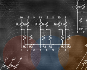
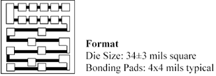
Santa Clara, CA – A global leader in Integrated Passives Devices (IPD), OnChip Devices today introduced a family of very small Thin Film Silicon wire-bondable Resistor Chips. These DR1212 resistor chips use sophisticated thin-film manufacturing process featuring a high-stability, self-passivating and moisture-resistant Tantalum Nitride resistor element. These chips offer 4 popular resistor values: 33, 100, 1K and 10K ohms. Additionally, these devices provide low shunt capacitance and low-noise operation which are ideal attributes for use in high performance hybrid microelectronics. The single value resistors have a very small die size of 12 x 12 mils sq and require two wire bonds. The Temperature Coefficient of Resistance (TCR) values as low as 25 ppm/°C.

The most common applications for these devices are termination and pull-up/pull-down. 100% electrically tested and visually inspected to MIL-STD-883, these silicon resistor chips feature resistance to thermal shock and high-temperature exposure. They are specified for an operating temperature range of –55°C to +125°C. Samples of all devices are available now, with lead times of 6 weeks for production quantities.

2x2_Array

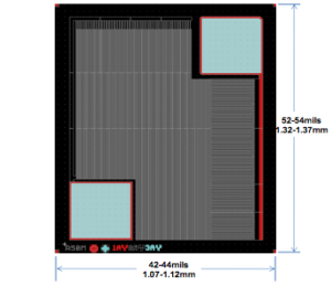
2×2 Array of 10K Ohm DR1212

Availability and Pricing
OnChip’s DR1212 resistor series is immediately available for purchase worldwide. These devices have production pricing in the range of $0.15 to $0.40, depending on volume and if the products are shipped on Mylar/Tape or in GelPaks/Waffle Packs. Samples are available immediately and standard lead time for production volume is 6 weeks upon receipt of order. Developed at the OnChip Santa Clara facility, these components are produced to the highest quality standards.

About OnChip Devices
OnChip Devices head-quartered in Santa Clara, CA is a global leader in Integrated Passive Devices. With its own silicon fabrication facility and strong partnerships with full turn-key assembly houses in Asia, OnChip is offering state-of-the-art silicon and ceramic solutions for High-brightness LED, Computing and Consumer Electronics.


OnChip Devices Introduces Ultra Low-Capacitance Integrated ESD Protection Chip for High-Speed Digital Interfaces

Superior Electrostatic Discharge Protection with Ultra-low Capacitance in Miniature Semiconductor Package now Available

Santa Clara, CA – OnChip Devices, Inc. today announced an ultra-low capacitance ESD (Electrostatic Discharge) protection chip to support high-speed data port applications. Available immediately, OnChip’s highly integrated ESD0504P solution provides a high-level of ESD protection for interfaces such as USB 3.0, Gbit Ethernet, Firewire, and HDMI.Shipped in very small foot-print UDFN package (1.6mm x 1.6mm x 0.6mm) the ESD0504P offers ultra-low line capacitance to ensure high signal integrity for video formats such as 1080p.

The ESD0504P chip delivers up to 8kV of ESD protection in contact discharge per IEC61000-4-2 standards for up to 4 channels. It also meets the IEC standard 61000-4-4 for EFT (Electrical Fast Transient) and CDE (Cable Discharge Events).With a low clamping voltage of 15V and a low capacitance of less than 1.5pF, the ESD0504P achieves a high level of ESD protection while maintaining signal quality for the latest generation of mobile electronics, with virtually no device degradation.

The ESD0504P is offered in a UDFN 6-Lead package to help PCB designers have flexibility in routing the transient current to the ground. A zener (TVS) diode is embedded between VP and VN to protect the VCC rail against ESD strikes and eliminates the need for a bypass capacitor (which would otherwise be needed for absorbing positive ESD strikes to ground).Furthermore, the chip’s design and it’s ultra-low line capacitance enables customers to improve time-to-market of their consumer products.

As portable electronics increase in capabilities (while maintaining their small size), ESD devices are becoming more prevalent in protecting passive elements on an IC board. OnChip Devices offers a large range of TVS diode products to minimize the risk of damage to electronic components. A low operating voltage allows for longer battery life, crucial in mobile electronics.

esd0504p

Availability and Pricing

The OnChip ESD0504P ESD protection chip offers 4-channels of ESD protection and is available immediately worldwide at US$0.15 in quantities of 10,000. Developed at OnChip Devices in the Santa Clara state-of-the-art facility, these ESD protection chips are produced to the highest quality standards.

About OnChip Devices

OnChip Devices headquartered in Santa Clara, CA is a global leader in Integrated Passive Devices. With its own silicon fabrication facility and strong partnerships with full turnkey assembly and test houses in Asia, OnChip is offering state-of-the-art silicon and ceramic solutions for High-brightness LED, Computing and Consumer Electronics.

OnChip Devices Introduces a Zener Diode Family That Offers the Highest Level of Electrostatic Discharge Protection Available in the Industry

With Outstanding ESD Protection Levels of Greater than 30kV Contact, OnChip’s ESD60x120 Silicon Zener Diodes are Available in Various Clamp Voltage Levels to Accommodate a Wide Range of Applications

Santa Clara, CA – OnChip Devices, a world leader in Integrated Passive Devices (IPD), has introduced miniature, wire-bondable, 1-channel silicon electrostatic discharge (ESD) protection diodes that are offered in various breakdown voltages. These ESD60x120 Zener diodes are Transient Voltage Suppressors that are available in seven breakdown voltage levels, which range from 6V to 40V with intermediate values of 8V, 13V, 14V, 20V, and 37V. They are designed with a very large single top-pad that simplifies wire-bonding. This large top-pad can potentially be used as a Chip Carrier targeted towards High Power LEDs, RF Circuits, Microwave Modules, and various other applications that require very high levels of ESD protection. The ESD60x120 diodes have a large cross-sectional area junction enabling the conduction of high transient currents. They provide superior electrical characteristics such as lower clamping voltage and exhibit literally no performance degradation when compared to Multilayer Varistors (MLV). All devices safely dissipate ESD strikes of over 30kV contact discharge per IEC-61000 International Standard, meet the stringent MIL-STD-883 conditions, and are in full RoHS compliance. When selecting the right Zener diode for ESD protection, engineers should ensure that the breakdown voltage of the ESD60x120 is larger than the Maximum Operating Voltage or Signal Amplitude of the circuit that needs to be protected.

“We are excited to launch a new silicon Zener diode family that offers the highest level of transient voltage protection available in the industry” said Ashok Chalaka, President and CEO. OnChip’s ESD60x120 diodes are 60 x 120 mils (1.5mm x 3mm) in size with a much smaller thickness ranging from only 4 mils to 12 mils (6, 8, and 10 mils also available). The ESD60x120 Zener diodes exhibit a breakdown voltage of up to 40V. They can be used for protecting a number of LEDs in a string ranging from 1 to 10 such as in RGB modules and other multi-chip modules. Protection from both positive and negative pulses (bidirectional signal) can also be possible by connecting two individual diodes with back-to-back topology.

ESD60x120_PR_Picture_Updated

High Brightness LEDs (HB LED) and High Power White LEDs using InGaN technology are manufactured to enable a market transition to energy efficient Solid-State Lighting (SSL). These LEDs continue to make major inroads into lighting applications that were conventionally dominated by incandescent light and other light sources. LEDs can be found in a wide array of applications ranging from traffic signals and automotive brake lights to full-color displays and LCD backlights. However, one of the main drawbacks of HB LED products is the fact that they are extremely sensitive to ESD. OnChip’s ESD60x120 diodes help to eliminate this weakness.

Availability and Pricing
The OnChip ESD60x120 diodes are available immediately worldwide at a unit price range of $0.19 to $0.45 depending on volumes and when shipped as undiced 5” wafers. They are also available as diced wafers on mylar/saw tape or in waffle packs for a slight price premium. These components are designed and developed at OnChip Devices’ Santa Clara facility and are produced to the highest quality standards.

About OnChip Devices
OnChip Devices is headquartered in Santa Clara, CA and is a global leader in Integrated Passive Devices. With its own silicon fabrication facility, strong partnerships with full turnkeys assembly, and test houses in Asia, OnChip is offering state-of-the-art silicon and ceramic solutions for High Brightness LED, Computing, and Consumer Electronics.

OnChip Introduces Capability to Design and Manufacture Custom Precision Thin Film Resistor Networks

OnChip Offers Quick-turn Custom Thin Film Resistor Arrays Ideal for High-Rel and Precision Applications

Santa Clara, CA – A global leader in Integrated Passives, OnChip Devices today announced the capability to design and manufacture custom Resistor Arrays with very short lead times. These Resistors can be specified by the customer and can include uncommon values, tight tolerances, and complex interconnections. These products can be available from concept to working samples in just a few weeks.

Design Engineers can mix and match resistor values to suit their exact application. The only specifications needed to get a custom network built by OnChip is to provide a schematic, resistor values, tolerances, and any special power or temperature coefficient requirements. These arrays can be built with tight ratio tolerances or matching between resistors. OnChip’s Thin Film Resistors feature greater electrical stability and higher precision while maintaining a miniature size. This is achieved by combining multiple Laser trimmable resistors on a single substrate, which requires less space than using discrete components. Resistors built on the same monolithic chip can have a wide range of different values and tolerances. With technology advancing rapidly, there is a pressing demand for systems to add more functionality and increase reliability while keeping the PC board compact. Thin Film Resistors cater to these critical needs. Furthermore, by incorporating custom resistor networks, the system adds an additional barrier to deter or prevent reverse engineering of the electronic hardware.

Custom_Resistor_Network_PR_8

OnChip’s custom resistor networks have numerous applications ranging from medical to instrumentation to high-end audio and video equipment to commercial avionics. Using advanced thin-film manufacturing techniques and featuring high-stability, self-passivating and moisture-resistant Tantalum Nitride resistor elements, these products make ideal precision Voltage Dividers. Applications include gain control of operational amplifiers, setting the voltage for high voltage regulators, attenuations and a level shifter for interfacing TTL/MOS. These resistor arrays are tested to stringent military standards associated with high performance electronic components and feature resistance to thermal shock and high-temperature exposure. In Addition to Tantalum Nitride, OnChip has the capability to produce Nickel Chrome and Silicon Chrome films for very high resistor values. While Silicon is the most common substrate these films are sputter deposited on, OnChip also offers Alumina and Aluminum Nitride for Resistors that are used in high power application. These products are offered as bare-die or in standard Semiconductor IC Packages such as SOT, SOIC, QSOP, MSOP, TSSOP and DIP. All devices are 100% electrically tested and products shipped as bare-die are visually inspected to MIL-STD-883. All of these devices are operational in the full military temperature range of –55°C to +125°C.

Availability and Pricing
The custom thin film resistance network capability is available immediately at a Non-recurring engineering (NRE) charges ranging from $2,500 to $6,500 depending on the design complexity of the device. Products are shipped either in wafer-form, bare-die or as packaged products and can be built in 4 to 8 weeks. These components are designed and developed at OnChip Devices’ Santa Clara facility and are produced to the highest quality standards. Please contact sales@onchip.com for a quote or additional information.

About OnChip Devices
OnChip Devices is headquartered in Santa Clara, CA and is a global leader in Integrated Passive Devices. With its own wafer fabrication facility and strong partnerships with full turn-keys assembly and test houses in Asia, OnChip is offering state-of-the-art silicon and ceramic solutions for High-Brightness LED, Computing, and Consumer Electronics.

OnChip Introduces Ultra Small ESD Protection Diodes with Extremely High Breakdown Voltage

Silicon Zener Diodes as Small as 7.9 x 7.9 mils sq and 4 mils (0.1mm) Thick Offer Exceptionally High Breakdown Voltage for High Brightness and Power LED Markets

Santa Clara, CA – OnChip Devices, a world leader in Integrated Passive Devices (IPD), has introduced miniature, wire bondable, silicon ESD (Electrostatic Discharge) protection diodes targeted for High Brightness and Power LED markets. The ESD7979 and ESD9595 diodes are designed with a junction, which enables conduction of high transient currents. These zeners exhibit no device degradation when compared to Multilayer Varistors (MLV). All devices meet the requirements of IEC61000 and safely dissipate ESD strikes of over 8kV when tested to the stringent MIL-STD-883 conditions.

High Brightness LEDs (HB LED) and High Power White LEDs using InGaN technology are manufactured to enable a market transition to energy efficient Solid-State Lighting (SSL). These LEDs continue to make major inroads into lighting applications that were traditionally dominated by incandescent light and other light sources. LEDs can be found in a wide array of applications ranging from traffic signals and automotive brake lights to full-color displays and LCD backlights. However, one of the main drawbacks of HB LED products is the fact that they are extremely sensitive to ESD. OnChip’s ESD7979 and ESD9595 diodes help to eliminate this weakness.

OnChip’s ESD7979 diode is only 7.9 x 7.9 mils (0.2mm x 0.2mm) in size with a thickness of 6 mils (0.15mm or 150um). The ESD9595 is slightly larger at 9.5 x 9.5 mils (0.24mm x 0.24mm) but with a thickness of only 4 mils (0.1mm or 100um). The tiny form-factor and single wire-bond feature make this device perfect for applications that have very confined spaces and miniature packaging. Though small in size these devices are manufactured to protect over 8kV of electrostatic discharge. A single high voltage ESD9595 has a zener diode voltage of 55V, whereas the ESD7979 diode exhibits a 100V breakdown voltage. They can be used for protecting a number of LEDs in a string ranging from 1 to 30 such as in RGB modules and other multi-chip modules. Protection from both positive and negative pulses (bidirectional signal) can also be possible by connecting two individual diodes with back-to-back topology.

OnChip also offers silicon and ceramic carriers or submounts that greatly improve the performance of HB LEDs.

Availability and Pricing
The OnChip ESD7979 and ESD9595 are available immediately worldwide at a price range of $0.02 to $0.03 USD in quantities of 100k to 150k units. They are available for shipment in wafer-form either diced or undiced. These components are designed and developed at OnChip Devices’ Santa Clara facility and are produced to the highest quality standards.

About OnChip Devices
OnChip Devices is headquartered in Santa Clara, CA and is a global leader in Integrated Passive Devices. With it’s own silicon fabrication facility and strong partnerships with full turn-keys assembly and test houses in Asia, OnChip is offering state-of-the-art silicon and ceramic solutions for High Brightness LED, Computing, and Consumer Electronics.

OnChip Introduces World’s Thinnest Capacitor

OnChip Has Developed a Very Thin (0.1mm) Silicon Based Dual-Capacitor Ideal for RFID Applications

Santa Clara, CA – OnChip Devices, a world leader in Integrated Passive Devices (IPD), has introduced a dual thin-film capacitor that is designed for Radio Frequency Identification (RFID) applications requiring both a tuning and a detuning capacitance in a single chip. OnChip’s DTCA chip features topside wire bonding pads to support either Chip-on-Board (COB) or Direct Chip Attachment (DCA) manufacturing flows. The chip uses a unique LPCVD (Low-Pressure Chemical Vapor Deposition) Silicon Nitride as the capacitor dielectric. This dielectric material offers high stability and Q values, exhibits low temperature and voltage coefficients, and achieves capacitance values in the range of 45pF to 165pF.

dtca pr small

0.1mm Dual Silicon Capacitor

By connecting the internal capacitors either individually, in series, or in parallel, the resonant frequency of the LC antenna circuit may easily be varied. As an example, if each capacitor value on the chip is 68pF, when these 2 caps are connected in series, the value will be 34pF and when connect in parallel, the value will be 136pF. The capacitance network is well suited for 13.56MHz ISO 15693 smart card applications, ISO 18000-3 RFID item management tags, and other applications that require precision, high frequency operation, and an ultra-thin profile. Intended to save space while providing superior electrical performance, OnChip’s DTCA dual capacitor chip is only 950um x 950um (37mils x 37mils or 0.95mm x 0.95mm) in size and is available as thin as 100um (4mils, 0.004″, or 0.1mm). The wire bondable top pad typically consists of aluminum, while the optional back metal is gold.

“Compared to conventional RF capacitors, OnChip’s DTCA capacitor offers extremely stable capacitance over a wide range of frequencies from 1MHz to several GHz. Additionally, their semiconductor construction provides an ultra-high Self-Resonant Frequency (SRF) and exceptionally low Equivalent Series Resistance (ESR)” said Ashok Chalaka, President and CEO. “Unlike Multi-layer Ceramic Capacitors (MLCC), DTCA offers an extremely repeatable frequency response due to the fact that the devices use a single-layer dielectric.” Typical applications for the dual capacitor chip include RFID resonance circuits and Chip-on-Board designs.

Availability and Pricing
The DTCA chip is available immediately worldwide at a price range of $0.07 to $0.15 USD (depending on capacitance value/tolerance and the chip thickness) in quantities of 10,000 units. Products are shipped in wafer-form (diced or undiced) and in waffle packs. These components are designed and developed at OnChip Devices’ Santa Clara facility and are produced to the highest quality standards.

About OnChip Devices
OnChip Devices is headquartered in Santa Clara, CA and is a global leader in Integrated Passive Devices. With it’s own silicon fabrication facility and strong partnerships with full turn-keys assembly and test houses in Asia, OnChip is offering state-of-the-art silicon and ceramic solutions for High-brightness LED, Computing, and Consumer Electronics.

OnChip Establishes New Capability to Provide Hi-Rel Visual Inspection Services for Wafers or Bare Die Semiconductors

OnChip is now offering 100% visual inspection for Intergated Circuits using both low and high power microscopes that meet commercial, military, and medical Electronics specifications

pr photo high power microscope-sm

Santa Clara, CA – OnChip has established new capability to offer 100% visual inspection using both low and high power microscopes that meet Commercial, Military and Medical Electronics specifications. Inspection is done to look for various types of visual defects.

Some of the more common defects include:

  • Embedded foreign material
  • Metallization or Passivation voids & irregularities
  • Contamination such as liquid or adhesive residues and surface particles
  • Surface scratches caused by test probes or wafer handlers
  • Dicing defects such as chip outs and cracks

Semiconductor ICs (Integrated Circuits) are extremely fragile and endure a variety of stresses during wafer fabrication, testing and dicing. They are easily prone to defects that would either prevent the device from operating correctly or pose a reliability concern for long-term operation. These defects are caused either during wafer fabrication or mechanically-induced during handling. The extent to which any defect may be acceptable would be defined by the appropriate criteria selected to fit the application environment. Units that are defective can be effectively removed by visually inspecting the devices under high magnification. There are many different inspection criteria, but the most common one is MIL-STD-883, Method 2010. This inspection standard defines the equipment to be used for the inspection, magnification ranges, what defects to look for and quantifies the amount of any particular defect that is acceptable.

The ability to visually inspect a circuit requires a lot of skill and training, which increases through experience and a continuous training program. OnChip employs a highly qualified staff of inspectors who have over 30 years of experience in this field. The company works very closely with customers during the initial phase to ensure proper calibration to the inspection needs. Visual inspection services are offered either in wafer-form or after the device has been sawn and placed in chip trays such as waffle packs or gel packs.

About OnChip Devices
OnChip Devices head-quartered in Santa Clara, CA is a global leader in Integrated Passive Devices. With an advanced silicon fabrication facility and strong partnerships with full turn-key assembly and test houses in USA as well as Asia, OnChip is offering state-of-the-art silicon and ceramic solutions for High-brightness LED, Computing, and Consumer Electronics.

OnChip Introduces the World’s Smallest High Meg-ohm Thin Film Resistors

OnChip Offers Resistors as high as 150 Meg-ohm in miniature silicon chips

Santa Clara, CA – OnChip, a global leader in Integrated Passive Devices (IPD), annouced the launch of highly sought-after Silicon based Thin Film components with resistance range of 5 Meg-ohms to 150 Meg-ohms. The XTM Resistor family is produced using OnChip’s proprietary processes and exhibit extreme stablity over the life of the product. This Thin Film process yields a resistance element that is also less noisy and more stable over extreme temperature when compared to Thick Film components available in the Industry.

There is a dire need for high value stable resistors for a variety of applications in Medical, Instrumentation, Mil-Aero markets and Consumer Electronics to improve performance as well as life of the battery powered devices. High Resistance precision chip resistors are essential for extremely low signal detection. They are also critical in Photodiode Signal Amplification, Photomultipliers, Ionization Detection and other Amplification Circuits. OnChip’s XTM devices with resistance as high as 150 Meg-ohm and small chip size of 44 mils x 54 mils are ideally suited for these stringent applications. The typical thickness of the device is 10 mils (250 micron). The top bond pads are large (13 x 13 mils sq) and are ideal for wire-bonding.

Screen Shot 2016-07-13 at 11.41.09 AM

World’s Smallest 150 Meg-ohm Silicon Resistor

“Designed with extremly long serpentine strings of high resistivity material these devices are built using Semiconductor Stepper Technology to achieve fine lines and space. Using advance Laser Systems the resistor links are trimmed to achieve any value between 5 Meg-ohm and 150 Meg-ohm” said Ashok Chalaka, President & CEO of OnChip Devices. The devices are built on 5″ wafers and can be shipped unsawn or sawn and in GelPaks. The operating temperature range is -55 to +175 degrees C. XTM’s stabilty over temperature is well below 500 ppm per degree C. This device can also be offered in miniature SMD IC packages such as SOT23 for Printed Circuit Board mounting.

Availability and Pricing
OnChip’s XTM can be laser trimmed to customer specific resistor values. Pricing varies depending on the resistor value and tolerance. Typical production unit price is $0.90. Pricing for SMD packaged units range between $1.50 and $1.85. Standard lead-time for this device is 4 to 6 weeks upon receipt of order. Developed at the OnChip Santa Clara facility, these components are produced to the highest quality standards.

About OnChip Devices
OnChip Devices head-quartered in Santa Clara, CA is a global leader in Integrated Passive Devices. With an advanced silicon fabrication facility and strong partnerships with full turn-key assembly and test houses in USA as well as Asia, OnChip is offering state-of-the-art silicon and ceramic solutions for High-brightness LED, Computing, and Consumer Electronics.

OnChip Introduces Submounts to Improve Efficiency of HB LED

OnChip Offers Silicon and Ceramic Carriers or Submounts that greatly improve the performance of High Brightness Light Emitting Diodes

Santa Clara, CA – A global leader in Integrated Passive Devices (IPD), OnChip today announced the ability to provide Silicon and Ceramic Carriers or Submounts for HB LED (High Brightness Light Emitting Diode) manufacturers. With major advantages of power savings, increased life expectancy and faster response time over traditional bulbs, HB LEDs are rapidly taking over many applications such as LCD backlighting, traffic lights, automotive lighting, camera flash and even standard lighting. HB LEDs are more efficient and longer lasting than both incandescent and CFLs.

HB LEDs are predominantly built with Indium Gallium Nitride (InGaN) technology. LEDs using InGaN come with several design challenges such as electrostatic discharge (ESD) sensitivity and package thermal coefficient of expansion (TCE) issues. InGaN chips are generally considered Class 1 devices and in many cases, a discharge of only 10 Volts can destroy such sensitive components. In comparison, static charge of up to 30,000 Volts is not uncommon and can be generated quite easily. Studies indicate that ESD damage to electronics and associated equipment is estimated at over $10 billion annually. ESD-damaged LEDs can appear dim, dead, shorted, or have low Vf or Vr. TCE mismatch between the LED chip and the lead-frame or package is another significant reliability threat. OnChip addresses both problems with these new submount offerings. OnChip produces silicon and ceramic submount that serves as an inter-poser between the InGaN chip and the lead-frame. Submounts reduce the TCE mismatch, while providing ESD protection via integrated zener diodes. Ceramics are ideal for High Power LEDs and OnChip offers both Aluminum Oxide and Aluminum Nitride materials. The Company also provides miniature silicon ESD diodes that can be mounted alongside the LED chips. These ESD diodes are available both as flip chips – ESD0201 and as single-wire bond chips – ESD-8×8. Submounts offer optical benefits as well. These devices contain solder bumps, enabling flip chip assembly of the LED chip. This approach eliminates shadows caused by wire-bonding. Furthermore, submounts offer a reflective metal surface which help direct the light in the desired direction.

Availability and Pricing
OnChip Silicon and Ceramic are typically built to customer specifications. Pricing varies depending on the size of the submount. Lead-time is 6 to 8 weeks upon receipt of order and customer’s final specifications. Developed at the OnChip Santa Clara facility, these components are produced to the highest quality standards. Please contact sales@onchip.com for a quote or additional information.

About OnChip Devices
OnChip Devices head-quartered in Santa Clara, CA is a global leader in Integrated Passive Devices. With an advanced silicon fabrication facility and strong partnerships with full turn-key assembly houses in Asia, OnChip is offering state-of-the-art silicon and ceramic solutions for High-brightness LED, Computing, and Consumer Electronics.

OnChip Introduces Thin Film Multi-tapped Silicon Chip Resistors for Hi-Rel Applications

OnChip Introduces an Extremely Versatile Designer Friendly Thin Film Wire-bondable Silicon Resistor Chips for Medical, Aerospace, Military, Communication, and Instrumentation Applications

110r image

Santa Clara, CA – A global leader in Integrated Passive Devices (IPD), OnChip today introduced a miniature Thin Film Silicon wire-bondable Resistor Chip that can offer a wide range of values. Using advanced thin-film manufacturing techniques and featuring high-stability, self-passivating and moisture-resistant Tantalum Nitride resistor elements, this product is ideal for developing quick-turn proto-types in the hybrid microelectronics labs. The multi-tapped 110R Series Resistors provide great flexibility to hybrid circuit designers. Consisting of a string of 20 resistors, these chips can be wire-bonded to offer a wide range of resistances. Measuring a size of 34 x 34 mils sq., the 110R consists of twenty one wire-bond pads. There are a set of 10 resistors with a value of 2.5k-ohms each and another set of 10 resistors with a value of 25k-ohms each, adding up to a total resistance of 275k-ohms. Since all these resistors are in series and with pads between each, the designer can get any values from 2.5k-ohms to 275k-ohms depending on what wire-bond pads are used. The 110R resistors offer TCR (Temperature Coefficient of Resistance) value as low as 250 ppm/°C. TCR Tracking between individual resistors are no more than 10 ppm/°C. . Additionally, these devices provide low shunt capacitance and low-noise operation which are ideal attributes for use in high performance hybrid microelectronics.

These silicon resistor chips feature resistance to thermal shock and high-temperature exposure. They are 100% electrically tested and visually inspected to MIL-STD-883. They are specified for an operating temperature range of -55°C to +125°C.

110R lower image


Availability and Pricing
The 110R thin film resistor chips are available immediately worldwide. These devices have production pricing in the range of $3.90 to $7.25, depending on the device tolerance and volume. While samples are available immediately, there is a lead-time of 6 weeks for production quantities. Developed at the OnChip Santa Clara facility, these components are produced to the highest quality standards.

About OnChip Devices
OnChip Devices head-quartered in Santa Clara, CA is a global leader in Integrated Passive Devices. With it’s own silicon fabrication facility and strong partnerships with full turn-key assembly houses in Asia, OnChip is offering state-of-the-art silicon and ceramic solutions for High-brightness LED, Computing and Consumer Electronics.