OnChip Announces Semiconductor Wafer Fabrication Services

A Wide Range of Wafer Foundry Services Are Available to Support Fabless Semiconductor Companies

Silicon manufacturing appears to have diminished in its luster and seems to be on the verge of extinction in Silicon Valley. The buzz today in the high tech capital of the world seems to be driven primarily by software companies; the likes of Facebook, Google, Intuit, Oracle, and LinkedIn. The traditional silicon chips seem to have stepped aside to give way for Big Data, Data Security, Mobile Apps, and Cloud Storage. The Valley which was traditionally recognized largely for its dominance in Semiconductors still boasts the highest concentration of companies involved in the design and development of silicon Integrated Circuits (ICs). However, much of the silicon wafer fabrication facilities have moved offshore, primarily to the Asia Pacific region. This has led to a score of serious risks such as loss of IP (intellectual property), lack of control over the production process, and the danger of finding these components in the gray market.

There are literally just a hand full of companies that have found a way to continue both innovating as well as “manufacturing” silicon products in Silicon Valley. OnChip Devices, Inc. is one such company that has successfully found a way to produce a wide range of silicon components in Santa Clara, CA. The company has announced that it is now offering wafer foundry services to fabless Semiconductor companies.

OnChip’s wafer foundry offers Thin Film, CMOS, and BiPolar processes and has produced more than 250 different high-volume products under the OnChip brand as well as for other companies globally. With installed capacity of over 10,000 wafers per month and current utilization of less than 30%, this state-of-the-art fab offers high quality wafers with competitive pricing and very short turnaround time. The fab produces 4”, 5”, and 6” wafers at 2µ to 5µ BiCMOS process technology focusing primarily on Analog products.

Large silicon wafer etching machine

OnChip’s wafer manufacturing facility has been granted the ISO 9001:2008 certification and strives to continuously improve its quality as well as the cycle time. The processing time for raw wafers is typically 6 to 8 weeks. With a workforce led by a very successful and long-tenured management team, the facility conducts frequent on-site trained maintenance for increased equipment uptime. In addition to silicon wafer fabrication, OnChip also offers various other services such as testing, dicing, and IC packaging.

Availability and Pricing
OnChip’s wafer foundry is committed to providing low cost non-recurring engineering (NRE) and setup charges, short lead-times, and high quality products and services. Please contact sales@onchip.com for a quote or additional information.

About OnChip Devices
OnChip Devices is headquartered in Santa Clara, CA and is a global leader in Integrated Passive Devices. With its own silicon fabrication facility and strong partnerships with full turn-keys assembly and test houses in Asia, OnChip is offering state-of-the-art silicon and ceramic solutions for High-brightness LED, Computing, and Consumer Electronics.

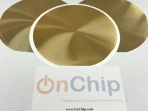
OnChip Offers a Full Service Silicon Wafer Backend Processing

OnChip’s Services Include Backgrinding, Back-metallization, Testing, Dicing, Die Loading, and Visual Inspection

Santa Clara, CA – A global leader in Integrated Passives, OnChip Devices today announced their onshore backend wafer processing. These services include Silicon wafer back-lap, various back-metal schemes, a wide range of wafer sort/test capabilities, sawing, die pick-and-place into waffle packs or gel packs, and final visual inspection.

Backgrinding

Backgrinding, lapping, or mechanical polishing are methods used to reduce thickness of wafers to attain a desired size (down to 100 microns or 4 mils) or surface texture (ultra fine finish of 2000-Grit). Proper backside surface finish is key to remove native oxide growth and ensure ideal back-metal adhesion. Our machines are capable of processing wafers ranging in size from 100 mm (4”) to 200 mm (8”). Standard lead-times are between 24-48 hours.

Back-metallization

OnChip’s systems deposit ultra-clean metal and dielectric films in a class-100 cleanroom. Generally, an in-situ RF etch is performed prior to sequential deposition of multilayers to insure good film adhesion and ohmic contact to underlying conductive layers or to the bare silicon. The most common metal stack consists of sputter deposited Titanium (500 Angstroms) followed by Nickel (3,000 Angstroms), and finally a flash of Gold (200 Angstroms).  All sputter films are currently available on silicon wafer sizes up to 150 mm (6”) in diameter. Larger wafer sizes may be considered on a case-by-case basis.

Testing

OnChip can process high volume while promising to deliver short lead-times and cut-rate (or competitive) prices. We offer both wafer probe (including bumped wafer probe) and final test. Our fully automatic wafer probers are capable of processing wafers up to 200 mm (8”). A wide range of automated test equipment allows for testing of analog, digital, mixed-signal and RF technologies with probers and handlers to support both wafer sort and package test. Multi-site wafer probing at hot temperature (up to 200°C) is available.

Dicing

OnChip’s dicing machines are capable of processing fragments and partial wafers to 200 mm (8”) silicon wafers. Additionally, other materials such as Gallium Arsenide, Micro-Electro-Mechanical systems (MEMS), and LEDs can also be processed. Dicing precision of less than 2 microns and kerf of less than 16 microns can be achieved.

Die Loading

OnChip offers both automated and manual loading of parts. Automated pick-and-place of die into packages including but not limited to gel packs and waffle packs. Manual pick-and-place via vacuum pen can also be requested for parts that are unpassivated, sensitive (moisture sensitive devices), MEMS, or require topside handling.

Visual Inspection

Semiconductor ICs (Integrated Circuits) are extremely fragile and endure a variety of stresses during wafer fabrication, testing, and dicing. They are easily prone to defects that would either prevent the device from operating correctly or pose a reliability concern for long-term operation. These defects are caused either during wafer fabrication or mechanically-induced during handling. OnChip has established capabilities to offer 100% visual inspection using both low and high power microscopes that meet Commercial, Military, and Medical Electronics specifications. Inspection is done to look for various types of visual defects. Some of the more common defects include:

  • Embedded foreign material
  • Metallization or Passivation voids & irregularities
  • Contamination such as liquid or adhesive residues and surface particles
  • Surface scratches caused by test probes or wafer handlers
  • Dicing defects such as chip outs and cracks

Availability and Pricing

All services are available immediately. These services are performed at OnChip Devices’ Santa Clara facility and are produced to the highest quality standards. Please contact sales@onchip.com for a quote or additional information.

About OnChip Devices

OnChip Devices is headquartered in Santa Clara, CA and is a global leader in Integrated Passive Devices. With its own silicon fabrication facility and strong partnerships with full turnkey assembly and test houses in USA & Asia, OnChip is offering state-of-the-art silicon and ceramic solutions for High Brightness LED, Computing, and Consumer Electronics.

OnChip Offers Semiconductor Wafer Backside Metallization

A Wide Range of Metal Stacks Are Offered to Improve Device Performance

Santa Clara, CA –  OnChip’s advanced wafer fabrication facility offers backside metallization (BSM) of thin films for various applications such as military, medical, and instrumentation. Back-metal is required on a wide range of Semiconductors devices to form a solderable die attach metal stack to ensure good electrical contact to the chip (ohmic contact) or proper bonding of the chips to their mounting cases. Power devices such as High Brightness Light Emitting Diodes (HB LED) require backside metal for an improved and reliable thermal conductivity. These metal layers are deposited using RF or DC sputtering and electron beam evaporation.

Silicon Wafers with Ti/Ni/Au Backside Metallization

Silicon Wafers with Ti/Ni/Au Backside Metallization

In backside metallization of discrete devices, the typical layer stack consists of three to four metal layers. The most common metal stack consists of sputter deposited Titanium (500 Angstroms) followed by Nickel (3,000 Angstroms), and finally a flash of Gold (200 Angstroms). Below is a list of all metals offered by OnChip:

Layers for providing good Ohmic Contact: Gold, Aluminum and Titanium
Barrier and superior Adhesion Layer: Copper, Chromium, Palladium and Titanium
Solder Layers: Nickel, Gold and Silver

OnChip’s systems deposit ultra-clean metal and dielectric films in a class-100 cleanroom. Generally, an in-situ RF etch is performed prior to sequential deposition of multilayers to insure good film adhesion and ohmic contact to underlying conductive layers or to the bare silicon. All sputter films are currently available on silicon wafer sizes up to 150mm (6”) in diameter. Larger wafer sizes may be considered on a case-by-case basis.

Availability and Pricing

The OnChip BSM processing is available immediately worldwide and the Lot Charge ranges from $750.00 to $1,450.00 (depending on metal stack, thickness of layers, wafer diameter, etc.). Typical lot size is 11 for 100mm (4”) wafers, 9 for 125mm (5”) wafers, and 7 for 150mm (6”) wafers. Typical lead times are 2 weeks ARO. The wafers are handled at OnChip Devices’ Santa Clara facility and are produced to the highest quality standards. Please contact sales@onchip.com for a quote or additional information.

About OnChip Devices

OnChip Devices is head-quartered in Santa Clara, CA and is a global leader in Integrated Passive Devices. With its own silicon fabrication facility and strong partnerships with full turn-keys assembly and test houses in Asia, OnChip is offering state-of-the-art silicon and ceramic solutions for High-brightness LED, Computing, and Consumer Electronics.

OnChip Adds Thin Film Resistor and R-C Capabilities for Customer Specific Applications

OnChip Offers Application Specific Semi-Custom and Full-Custom Precision Silicon Resistors and Resistor-Capacitor Networks

Santa Clara, CA – A global leader in Integrated Passives, OnChip Devices today announced the ability to develop and build semi-custom and full-custom Silicon based Resistor and Resistor-Capacitor Arrays using its proprietary Thin Film Process Technology. The circuit schematic can be Application specific and can include a wide range of resistor and capacitor values, tight resistor tolerances, and complex interconnections. These arrays can be manufactured from design concept to working samples in less than 8 weeks.

Customers can replace discrete Resistors and Capacitors into a single monolithic silicon circuit to match their product needs. These R and R-C arrays can provide significant cost as well as PCB board-space savings. OnChip’s proprietary Thin Film Process offers Resistors featuring superior electrical stability and higher precision while maintaining a miniature size.

Features:

  • Resistances from 1 Ohm to 100MegOhm

           o Tight tolerances to 0.1%, precision matching, high stability, and low TCR, VCR
           o Exceptional voltage and power handling capabilities

  • Capacitors ranging from 2pF to 2,000pF

Applications:

  • System in Package (SIP)
  • RF/Communication
  • Medical
  • Scientific
  • Industrial
  • Military

These products are offered as bare-die or in standard Semiconductor IC Packages such as SC70, SOT, TDFN, uDFN, SOIC, QSOP, MSOP, TSSOP and DIP. All devices are 100% electrically tested and products shipped as bare-die are visually inspected to MIL-STD-883. All of these devices are operational in the full military temperature range of –55°C to +125°C.

Availability and Pricing

The custom thin film resistance network capability is available immediately at a Non-recurring engineering (NRE) charges ranging from $4,500 to $7,500 depending on the design complexity of the device. Products are shipped either in wafer-form, bare-die or as packaged products and can be built in 6 to 8 weeks. These components are designed and developed at OnChip Devices’ Santa Clara facility and are produced to the highest quality standards.

About OnChip Devices

OnChip Devices is headquartered in Santa Clara, CA and is a global leader in Integrated Passive Devices. With its own silicon fabrication facility and strong partnerships with full turnkey assembly and test houses in Asia, OnChip is offering state-of-the-art silicon and ceramic solutions for High Brightness LED, Computing, and Consumer Electronics.

OnChip Devices Releases New Line of TVS diodes in Through Hole and Surface Mount Packages

New TVS diodes have quick lead-time and come in standard discrete packages

Santa Clara, CA OnChip Devices announces the release of new TVS diodes for PC boards that use standard thru hole or surface mount technology. TVS diodes are designed for voltage suppression in a circuit that is susceptible to electrostatic discharge (ESD). It protects various circuit components by providing a low impedance path for transient current to travel through, redirecting the dangerous currents to ground. These TVS diodes range from 5V up to 440V, providing a solution for a variety of projects. Some applications include consumer electronics, military, communications, LED, and the automotive industry. The new TVS diodes are available in glass axial packages as well as plastic surface mount packages, and are lead-free and RoHS compliant.

TopDiode_TVS_picture

The SMJC Diode is Assembled into a DO214AC (SMC) 2 Lead Surface Mount Package

The KE series offers exceptional protection from pulse currents up to 140A. It also offers the designer up to 1500W of power dissipation. These are available in DO axial glass packages, with the option of unidirectional or bidirectional signal protection. The SM series comes in a two lead DO214 surface mount package. It has a large cross junction for high power dissipation of up to 1500W. This series is also available in a unidirectional or bidirectional configuration, with various options for device tolerance. The plastic package is ideal for mass manufactured board that utilize pick and place automation. All of these diodes are designed for suppressing unwanted voltage spikes that can cause damage to other valuable circuit elements.

Availability and Pricing

These new TVS diodes are in stock and available for immediate delivery. High volume demands can be shipped within a few weeks. The products offer very competitive pricing. Please contact factory for additional details.

About OnChip Devices

OnChip Devices is headquartered in Santa Clara, CA and is a global leader in Integrated Passive Devices. With its own silicon fabrication facility and strong partnerships with full turnkey assembly and test houses in Asia, OnChip is offering state-of-the-art silicon and ceramic solutions for High Brightness LED, Computing, and Consumer Electronics.
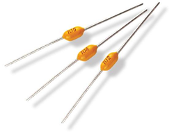
OnChip Devices Unveils New Line of Zener diodes in Through Hole and Surface Mount Packages

New Zener diodes provide protection for low voltage applications in standard discrete packages

Santa Clara, CA – OnChip Devices announces the expansion of its Zener diodes, increasing package options to include common discrete parts. Zener diodes are implemented to protect valuable circuit elements from being destroyed by harmful voltage surges resulting from electrostatic discharge. Ranging from 2V to 100V, these Zeners can be used for voltage regulation in a variety of applications such as consumer electronics, military, communications, LED, and automotive industries. These Zener diodes are available in axial, MELF, and plastic surface mount packages that are Pb-free and comply with the RoHS directive.

TopDiode_Zener_picture

BZX84C Series Zener in a SOT23 3 Lead Surface Mount Package

These Zeners are available with tolerances of +/- 1% and leakage current as low as 0.05uA. They are rated for use in high temperature environments up to 200°C. Breakdown voltage and power dissipation are consistent when tested to varying current values, providing the designer with predictable electrical behavior for each specific application. The 1N47 glass diodes have low Zener impedance and provide power dissipation of 1000mW in an axial JEDEC DO-41 package. The ZM47 series provides the same electrical characteristics of the 1N47 series in a glass case MELF package. The BZX55C glass diode series have low leakage current of 0.1uA and a low regulation factor, which ensures the input current through the diode does not deviate noticeably from the output current. The BZV55C series is electrically equivalent to the BZX55C series, but comes in a mini MELF package instead of an axial JEDEC DO-35 package. The BZX84C series is offered in the standard SOT23-3 package. This package is good for automated pick and place assembly for mass produced PC boards. The BZX84C series also has low reverse current, ideal for low voltage applications. All of these diodes are designed to function as voltage regulators, providing constant output voltage regardless of the surges of voltage from the power supply or ESD discharge.

Availability and Pricing

These new TVS diodes are in stock and available for immediate delivery. High volume demands can be shipped within a few weeks. The products offer very competitive pricing. Please contact factory for additional details.

About OnChip Devices

OnChip Devices is headquartered in Santa Clara, CA and is a global leader in Integrated Passive Devices. With its own silicon fabrication facility and strong partnerships with full turnkey assembly and test houses in Asia, OnChip is offering state-of-the-art silicon and ceramic solutions for High Brightness LED, Computing, and Consumer Electronics.
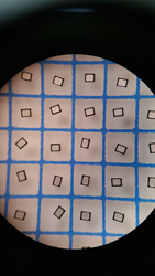
OnChip Devices Unveils New Line of Electrolytic Capacitors for Thru-hole and Surface-mount PC Boards

The addition of electrolytic and tantalum bead capacitors to OnChip’s product line offers high capacitance in small sizes

Santa Clara, CA – OnChip added a wide range of devices to its capacitor product-line. Additions include axial, radial, surface mount, and V-chip film capacitors. These new devices expand OnChip’s previous line of capacitors by offering solutions for PCB designers who do not use wire bondable die in their circuits. These parts are moisture resistant and rated for DC circuits anywhere from 4V up to 2000V. All of OnChip’s capacitors are Pb-free and comply to the RoHS directive.

gI_115817_20128291428484681

Axial capacitors

OnChip’s new capacitors are available with a variety of dielectric materials. The CA series is a tantalum bead capacitor available in radial thru-hole or surface-mount packages. Tantalum capacitors are ideal for applications that require high capacitance but have limited board space. The CBB series features a polypropylene dielectric that provides a dissipation factor of <0.002, as well as providing consistent capacitance values for applications with fluctuating frequencies. The CL series is built with polyester and is incredibly stable for long-term usage. CL capacitors feature a precise tolerance as tight as 1%. The CT series is a ceramic capacitor with options for different dielectrics such as NPO, X7R, Z5U, and Y5V. NPO is recommended in applications where capacitance value needs to be stable in varying temperature, frequency, and voltage. X7R, Z5U, and Y5V have predictable properties that can be used to manipulate the capacitor’s capabilities when subjected to these same variations. The TC series of V-Chip Capacitors provide a surface mount option that is good for ripple currents and switching power supplies. They are built to withstand high voltages and protect sensitive parts on the PCB in the event of a short circuit. All capacitors have a rated load life determined by the hours that they can function at maximum operating temperature, while maintaining their electrical characteristics.

Availability and Pricing

These new capacitors are in stock and available for immediate delivery. High volume demands can be shipped within a few weeks. The products offer very competitive pricing. Please contact factory for additional details.

About OnChip Devices

OnChip Devices is headquartered in Santa Clara, CA and is a global leader in Integrated Passive Devices. With its own silicon fabrication facility and strong partnerships with full turnkey assembly and test houses in Asia, OnChip is offering state-of-the-art silicon and ceramic solutions for High Brightness LED, Computing, and Consumer Electronics.

OnChip Introduces Low Voltage Diodes for High-Brightness LED Protection

OnChip’s Low Voltage Zener Chips Protect High Brightness Light Emitting Diodes from Damage Caused by Transient Voltages and Electrostatic Discharge

Santa Clara, CA – OnChip Devices, a world leader in Integrated Passive Devices (IPD), has introduced a wire-bondable silicon ESD diode chip targeted towards low voltage LED applications. Adding to its broad range of bare-die diode offerings, these Zeners are ideal for protecting circuits by suppressing voltage higher than 3.0 Volts. The ESD2117 diode can handle pulses of up to 350W and 20A, providing protection of 8kV when tested to level 4 of the IEC 61000-4-2 standard. These diodes do not exhibit any device degradation when compared to Multilayer Varistors (MLV). ESD2117 chip diodes are lead-free and RoHS compliant.

High Brightness LEDs (HB LED) and High Power White LEDs are enabling a market transition to energy efficient Solid-State Lighting (SSL). However, LED products are extremely sensitive to electrostatic discharge (ESD) as well as transient voltages. By introducing a Zener diode into the circuit, the LED is protected from surges in voltage that can cause permanent damage. Using a Zener diode is a preventive method to ensure that time and money are saved in the lifespan of the application.

The ESD2117 chip can also be used in multi-chip, RF, and Hybrid microelectronics modules. The small chip size and single wire bond pad make this device ideal for applications with limited board space. A large cross-sectional area of the N-P junction allows the device to conduct high transient currents.

gI_114720_ESD2117 GelPak

ESD2117 diodes are available in a variety of different formats including Gel-Paks (shown above)

The ESD2117 is a 21 x 17 mils chip with 7.5 mil thickness. The top bond pad is large (15 x 11 mils) for easy wire bonding. The chip’s silver back metal allows direct placement onto PCBs, saving space while ensuring high electrical conductivity for a fraction of the cost of gold. Placing two of these diodes back to back will protect the circuit from both AC and DC voltage spikes.

Availability and Pricing
OnChip’s ESD2117 diodes are available immediately in the US and international markets. They can be shipped in undiced 4” wafers (31k units), diced on Mylar tape, or placed in Gel-Paks or Waffle Packs. ESD2117 diodes are designed and manufactured at OnChip Devices’ Santa Clara facility in California, and produced to the highest quality standards.

About OnChip Devices
OnChip Devices is headquartered in Santa Clara, CA and is a global leader in Integrated Passive Devices. With its own silicon fabrication facility and strong partnerships with full turnkey assembly and test houses in Asia, OnChip is offering state-of-the-art silicon and ceramic solutions for High Brightness LED, Computing, and Consumer Electronics.

OnChip Introduces New Series of Space Saving Bare-die Zener Diodes for Transient Voltage Suppression

Silicon ESD Zener Diodes as small as 8×8 mils sq and 4 mils thick offer protection for High-Brightness LED and Multi-chip Module applications

Santa Clara, CA – OnChip Devices, a world leader in Integrated Passive Devices (IPD), has introduced miniature, wire bondable, silicon ESD (Electrostatic Discharge) protection diodes targeted for High Brightness and Power LED markets. The ESD88NP and ESD88PN are designed to redirect high transient currents away from sensitive LED and IC products. These Zeners exhibit no device degradation when compared to Multilayer Varistors (MLV). All devices meet the requirements of IEC61000 and safely dissipate ESD strikes of over 8kV when tested to the stringent MIL-STD-883 conditions. These products are Pb-free and conform to all RoHS requirements.

OnChip’s ESD88 diodes are ideal for computers, TVs, LEDs, medical instruments, and portable electronics. They work to protect over-voltage on I/O and power lines, protecting any downstream components. High Brightness LEDs (HB LED) and High Power White LEDs using InGaN technology are manufactured to enable a market transition to energy efficient Solid-State Lighting (SSL). These LEDs continue to make major inroads into lighting applications that were conventionally dominated by incandescent light and other light sources. LEDs can be found in a wide array of applications ranging from traffic signals and automotive brake lights to full-color displays and LCD backlights. However, one of the main drawbacks of HB LED products is the fact that they are extremely sensitive to ESD. OnChip’s ESD88 diodes help to eliminate this weakness.

The ESD88 series features an 8 x 8 mils sq chip size with an option for either 4 or 6 mil thickness. They are available with a variety of breakdown voltages such as 5, 7, 10, and 13V.The ESD88NP has a wire bondable cathode top pad and anode bottom, while the ESD88PN features a wire bondable anode and cathode bottom. The small chip size is ideal for protecting sophisticated Multi-chip Modules (MCM) and System-on-a-chip (SoC) applications. Protection from positive and negative voltage surges (AC signals) can be made possible by connecting two diodes back to back.

Availability and Pricing
OnChip’s ESD88NP and ESD88PN diodes are available immediately worldwide. They can be shipped as undiced 5” wafers, diced on Mylar tape as well as in GelPaks/Waffle Packs. These devices sell in the price range of $0.06 to $0.09 in production volumes and when shipped on tape. These components are designed and developed at OnChip Devices’ Santa Clara facility and are produced to the highest quality standards.

About OnChip Devices
OnChip Devices is headquartered in Santa Clara, CA and is a global leader in Integrated Passive Devices. With its own silicon fabrication facility and strong partnerships with full turnkey assembly and test houses in Asia, OnChip is offering state-of-the-art silicon and ceramic solutions for High Brightness LED, Computing, and Consumer Electronics.

OnChip Introduces a New Family of Flip Chip Resistors for Consumer Electronics Application

The FCRN family is a series of Thin Film Resistors built with moisture resistant Tantalum Nitride for durability, long term stability and offers extremely tight tolerances

Santa Clara, CA – OnChip Devices announces a new family of high precision space saving flip-chip resistors. By using sophisticated thin film manufacturing technology and advanced laser trim systems, the FCRN family offers precise resistance values for applications with limited PCB space. These resistors typically range from 10Ω – 500Ω with tolerance as tight as ±0.1%. FCRN flip-chips are designed to mount according to IPC-7351 SMD and Land Pattern Standard. Each resistor is manufactured with moisture-resistant tantalum nitride and bumped with lead-free eutectic SnAgCu (SAC) alloy for RoHS-compliance. These chips are built for applications that allow resistors to be mounted on external circuitry by means of solder reflow. Flip-chips allow for SMT to move away from through-hole technology, helping to dramatically increase the PC Board density.

Shawn Merchant, Applications Engineer at OnChip Devices said, “Flip-chip resistors save space by reducing the size of the land pattern as compared to resistors with wraparound terminals. TCR (Temperature Coefficient of Resistance) values for the FCRN family are stable and as low as 25 ppm/°C for a wide temperature range from -55°C to 155°C.” With low noise and extremely precise tolerances, these resistors are ideal for medical, instrumentation, mil-aero and consumer electronics applications.

The FCRN306 chip is a 1 channel resistor in a size 0603 flip chip. It is built with a ceramic substrate and tantalum nitride resistor material. The solid ceramic substrate creates a seal around the resistor material to prevent moisture penetration. This 2 lead flip chip has a pitch of 1.2mm.

FCRN306

FCRN306

The FCRN312 chip is a 4 channel resistor network in a 0603 silicon package with a 0.4mm pitch. These resistors are available with an optional ratio match of ±0.05% for precision and tolerance of ±0.1% for accuracy.

FCRN312_picture

FCRN312

The FCRN317 chip is a 1 channel resistor in a ceramic 0805 package with a 1.5mm pitch. Ceramic substrates are ideal for their ability to withstand high voltage pulses and provide thermal resistance from the beginning of the manufacturing process to the end life of the product.

FCRN317

FCRN317


Availability and Pricing

OnChip’s FCRN resistors can be laser trimmed to different resistor values. Non-standard values are also available. Pricing varies based on tolerance and TCR values. Samples are available immediately and production volume lead time is 6 weeks upon receipt of order.

About OnChip Devices

OnChip Devices head-quartered in Santa Clara, CA is a global leader in Integrated Passive Devices. With its own silicon fabrication facility and strong partnerships with full turn-key assembly houses in Asia, OnChip is offering state-of-the-art silicon and ceramic solutions for High-brightness LED, Computing and Consumer Electronics.